日本語
日本語


 人気検索:
人気検索:
 (0)
(0)
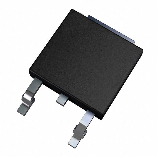
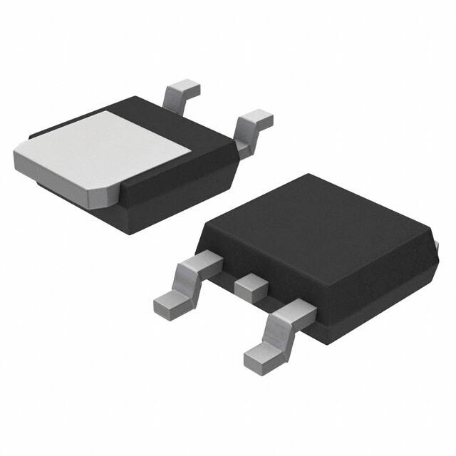
画像はあくまで参考です。


FDD8878
-
ON Semiconductor

-
Transistors - FETs, MOSFETs - Single
- TO-252-3, DPak (2 Leads + Tab), SC-63
- Trans MOSFET N-CH 30V 11A 3-Pin(2 Tab) DPAK T/R
 Date Sheet
在庫數 100000
- 1+: $0.65066
- 10+: $0.61383
- 100+: $0.57908
- 500+: $0.54630
- 1000+: $0.51538
小計金額 $0.65066
仕様 よくある質問
- Lifecycle Status:ACTIVE (Last Updated: 1 day ago)
- Factory Lead Time:10 Weeks
- Contact Plating:Tin
- Mount:Surface Mount
- Mounting Type:Surface Mount
- Package / Case:TO-252-3, DPak (2 Leads + Tab), SC-63
- Number of Pins:3
- Weight:260.37mg
- Transistor Element Material:SILICON
- Current - Continuous Drain (Id) @ 25℃:11A Ta 40A Tc
- Drive Voltage (Max Rds On, Min Rds On):4.5V 10V
- Number of Elements:1
- Power Dissipation (Max):40W Tc
- Turn Off Delay Time:38 ns
- Operating Temperature:-55°C~175°C TJ
- Packaging:Tape & Reel (TR)
- Series:PowerTrench®
- Published:2005
- JESD-609 Code:e3
- Pbfree Code:yes
- Part Status:Active
- Moisture Sensitivity Level (MSL):1 (Unlimited)
- Number of Terminations:2
- ECCN Code:EAR99
- Voltage - Rated DC:30V
- Terminal Form:GULL WING
- Current Rating:40A
- JESD-30 Code:R-PSSO-G2
- Element Configuration:Single
- Operating Mode:ENHANCEMENT MODE
- Power Dissipation:40W
- Case Connection:DRAIN
- Turn On Delay Time:7 ns
- FET Type:N-Channel
- Transistor Application:SWITCHING
- Rds On (Max) @ Id, Vgs:15m Ω @ 35A, 10V
- Vgs(th) (Max) @ Id:2.5V @ 250μA
- Input Capacitance (Ciss) (Max) @ Vds:880pF @ 15V
- Gate Charge (Qg) (Max) @ Vgs:26nC @ 10V
- Rise Time:79ns
- Vgs (Max):±20V
- Fall Time (Typ):27 ns
- Continuous Drain Current (ID):40A
- Threshold Voltage:1.2V
- JEDEC-95 Code:TO-252AA
- Gate to Source Voltage (Vgs):20V
- Drain to Source Breakdown Voltage:30V
- Avalanche Energy Rating (Eas):25 mJ
- Height:2.39mm
- Length:6.73mm
- Width:6.22mm
- REACH SVHC:No SVHC
- Radiation Hardening:No
- RoHS Status:ROHS3 Compliant
- Lead Free:Lead Free


 サポートセンター
 購入サービス
 プライバシーと規約
 Kynix について
 お問合せ
お問合せ